 |
| October 13, 2020 | Volume 16 Issue 39 |
Mechanical News & Products

Designfax weekly eMagazine

Archives
Partners
Manufacturing Center
Product Spotlight
Modern Applications News
Metalworking Ideas For
Today's Job Shops
Tooling and Production
Strategies for large
metalworking plants
hyperMILL 2024 CAD/CAM software suite
 OPEN MIND Technologies has introduced its latest hyperMILL 2024 CAD/CAM software suite, which includes a range of powerful enhancements to its core toolpath capabilities, as well as new functionality for increased NC programming efficiency in applications ranging from 2.5D machining to 5-axis milling. New and enhanced capabilities include: Optimized Deep Hole Drilling, a new algorithm for 3- and 5-axis Rest Machining, an enhanced path layout for the 3D Plane Machining cycle, better error detection, and much more.
Learn more.
One-part epoxy changes from red to clear under UV
 Master Bond UV15RCL is a low-viscosity, cationic-type UV-curing system with a special color-changing feature. The red material changes to clear once exposed to UV light, indicating that there is UV light access across the adhesive material. Although this change in color from red to clear does not indicate a full cure, it does confirm that the UV light has reached the polymer. This epoxy is an excellent electrical insulator. UV15RCL adheres well to metals, glass, ceramics, and many plastics, including acrylics and polycarbonates.
Learn more.
SPIROL Press-N-Lok™ Pin for plastic housings
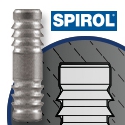 The Press-N-Lok™ Pin was designed to permanently retain two plastic components to each other. As the pin is inserted, the plastic backfills into the area around the two opposing barbs, resulting in maximum retention. Assembly time is quicker, and it requires lower assembly equipment costs compared to screws and adhesives -- just Press-N-Lok™!
Learn more about the new Press-N-Lok™ Pin.
Why hybrid bearings are becoming the new industry standard
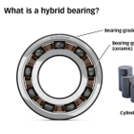 A combination of steel outer and inner rings with ceramic balls or rollers is giving hybrid bearings unique properties, making them suitable for use in a wide range of modern applications. SKF hybrid bearings make use of silicon nitride (twice as hard as bearing steel) rolling elements and are available as ball bearings, cylindrical roller bearings, and in custom designs. From electric erosion prevention to friction reduction and extended maintenance intervals, learn all about next-gen hybrid bearings.
Read the SKF technical article.
3M and Ansys train engineers on simulating adhesives
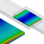 Ansys and 3M have created an advanced simulation training program enabling engineers to enhance the design and sustainability of their products when using tapes and adhesives as part of the design. Simulation enables engineers to validate engineering decisions when analyzing advanced polymeric materials -- especially when bonding components made of different materials. Understand the behavior of adhesives under real-world conditions for accurate modeling and design.
Read this informative Ansys blog.
New FATH T-slotted rail components in black from AutomationDirect
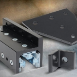 Automation-Direct has added a wide assortment of black-colored FATH T-slotted hardware components to match their SureFrame black anodized T-slotted rails, including: cube connectors (2D and 3D) and angle connectors, joining plates of many types, brackets, and pivot joints. Also included are foot consoles, linear bearings in silver and black, cam lever brakes, and L-handle brakes. FATH T-slotted hardware components are easy to install, allow for numerous T-slotted structure configurations, and have a 1-year warranty against defects.
Learn more.
Weird stuff: Moon dust simulant for 3D printing
 Crafted from a lunar regolith simulant, Basalt Moon Dust Filamet™ (not a typo) available from The Virtual Foundry closely mirrors the makeup of lunar regolith found in mare regions of the Moon. It enables users with standard fused filament fabrication (FFF) 3D printers to print with unparalleled realism. Try out your ideas before you go for that big space contract, or help your kid get an A on that special science project.
Learn more.
Break the mold with custom injection molding by Rogan
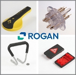 With 90 years of industry experience, Rogan Corporation possesses the expertise to deliver custom injection molding solutions that set businesses apart. As a low-cost, high-volume solution, injection molding is the most widely used plastics manufacturing process. Rogan processes include single-shot, two-shot, overmolding, and assembly. Elevate your parts with secondary operations: drilling and tapping, hot stamping, special finishes, punch press, gluing, painting, and more.
Learn more.
World's first current-carrying fastening technology
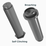 PEM® eConnect™ current-carrying pins from Penn-Engineering provide superior electrical connections in applications that demand high performance from internal components, such as automotive electronics. This first-to-market tech provides repeatable, consistent electrical joints and superior installation unmatched by traditional fastening methods. Features include quick and secure automated installation, no hot spots or poor conductivity, and captivation options that include self-clinching and broaching styles.
Learn more about eConnect pins.
New interactive digital catalog from EXAIR
 EXAIR's latest catalog offers readers an incredible source of innovative solutions for common industrial problems like conveying, cooling, cleaning, blowoff, drying, coating, and static buildup. This fully digital and interactive version of Catalog 35 is designed for easy browsing and added accessibility. Customers can view, download, print, and save either the full catalog or specific pages and sections. EXAIR products are designed to conserve compressed air and increase personnel safety in the process. Loaded with useful information.
Check out EXAIR's online catalog.
5 cost-saving design tips for CNC machining
 Make sure your parts meet expectations the first time around. Xometry's director of application engineering, Greg Paulsen, presents five expert tips for cutting costs when designing custom CNC machined parts. This video covers corners and radii, designing for deep pockets, thread depths, thin walls, and more. Always excellent info from Paulsen at Xometry.
View the video.
What can you secure with a retaining ring? 20 examples
 From the watch dial on your wrist to a wind turbine, no application is too small or too big for a Smalley retaining ring to secure. Light to heavy-duty loads? Carbon steel to exotic materials? No problem. See how retaining rings are used in slip clutches, bike locks, hip replacements, and even the Louvre Pyramid.
See the Smalley design applications.
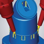
Load fasteners with integrated RFID
 A crane, rope, or chain may be required when something needs lifting -- plus anchoring points on the load. JW Winco offers a wide range of solutions to fasten the load securely, including: lifting eye bolts and rings (with or without rotation), eye rings with ball bearings, threaded lifting pins, shackles, lifting points for welding, and more. Some, such as the GN 581 Safety Swivel Lifting Eye Bolts, even have integrated RFID tags to clearly identify specific lifting points during wear and safety inspections and manage them digitally and without system interruption.
Learn more.
Couplings solve misalignments more precisely with targeted center designs
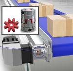 ALS Couplings from Miki Pulley feature a simplistic, three-piece construction and are available in three different types for more precisely handling parallel, angular, or axial misalignment applications. The key feature of this coupling design is its center element. Each of the three models has a center member that has a unique and durable material and shape. Also called a "spider," the center is designed to address and resolve the type of misalignment targeted. Ideal for unidirectional continuous movement or rapid bidirectional motion.
Learn more.
What is 3D-MID? Molded parts with integrated electronics from HARTING
 3D-MID (three-dimensional mechatronic integrated devices) technology combines electronic and mechanical functionalities into a single, 3D component. It replaces the traditional printed circuit board and opens up many new opportunities. It takes injection-molded parts and uses laser-direct structuring to etch areas of conductor structures, which are filled with a copper plating process to create very precise electronic circuits. HARTING, the technology's developer, says it's "Like a PCB, but 3D." Tons of possibilities.
View the video.
MIT tries turning diamond metallic to make next-gen semiconductor

Researchers have discovered a way to transform the electronic properties of nanoscale needles of diamond. [Image: MIT News]
Long known as the hardest of all natural materials, diamonds are also exceptional thermal conductors and electrical insulators. Now, researchers have discovered a way to tweak tiny needles of diamond in a controlled way to transform their electronic properties, dialing them from insulating, through semiconducting, all the way to highly conductive, or metallic. This can be induced dynamically and reversed at will, with no degradation of the diamond material.
The research, though still at an early proof-of-concept stage, may open up a wide array of potential applications, including new kinds of broadband solar cells, highly efficient LEDs and power electronics, and new optical devices or quantum sensors, the researchers say.
Their findings, which are based on simulations, calculations, and previous experimental results, are reported in the Proceedings of the National Academy of Sciences in October 2020. The paper is by MIT Professor Ju Li and graduate student Zhe Shi; Principal Research Scientist Ming Dao; Professor Subra Suresh, who is president of Nanyang Technological University in Singapore as well as former dean of engineering and Vannevar Bush Professor Emeritus at MIT; and Evgenii Tsymbalov and Alexander Shapeev at the Skolkovo Institute of Science and Technology in Moscow.
The team used a combination of quantum mechanical calculations, analyses of mechanical deformation, and machine learning to demonstrate that the phenomenon, long theorized as a possibility, really can occur in nanosized diamond.
The concept of straining a semiconductor material such as silicon to improve its performance found applications in the microelectronics industry more than two decades ago. However, that approach entailed small strains on the order of about 1%. Li and his collaborators have spent years developing the concept of elastic strain engineering. This is based on the ability to cause significant changes in the electrical, optical, thermal, and other properties of materials simply by deforming them -- putting them under moderate to large mechanical strain, enough to alter the geometric arrangement of atoms in the material's crystal lattice, but without disrupting that lattice.
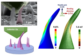
Tiny needles of diamond are strained by bending, as seen in this electron microscope image, top left. Computer simulations show the effects, with normal insulating properties in green, and areas with metallic properties, never seen before in diamond, in deep red. [Image: Courtesy of the researchers. Edited by MIT News]
In a major advance in 2018, a team led by Suresh, Dao, and Yang Lu from the City University of Hong Kong showed that tiny needles of diamond, just a few hundred nanometers across, could be bent without fracture at room temperature to large strains. They were able to repeatedly bend these nanoneedles to tensile strain as much as 10%; the needles can then return intact to their original shape.
Key to this work is a property known as bandgap, which essentially determines how readily electrons can move through a material. This property is thus key to the material's electrical conductivity. Diamond normally has a very wide bandgap of 5.6 electron volts, meaning that it is a strong electrical insulator that electrons do not move through readily. In their latest simulations, the researchers show that diamond's bandgap can be gradually, continuously, and reversibly changed, providing a wide range of electrical properties, from insulator through semiconductor to metal.
"We found that it's possible to reduce the bandgap from 5.6 electron volts all the way to zero," Li says. "The point of this is that if you can change continuously from 5.6 to 0 electron volts, then you cover all the range of bandgaps. Through strain engineering, you can make diamond have the bandgap of silicon, which is most widely used as a semiconductor, or gallium nitride, which is used for LEDs. You can even have it become an infrared detector or detect a whole range of light all the way from the infrared to the ultraviolet part of the spectrum."
"The ability to engineer and design electrical conductivity in diamond without changing its chemical composition and stability offers unprecedented flexibility to custom design its functions," says Suresh. "The methods demonstrated in this work could be applied to a broad range of other semiconductor materials of technological interest in mechanical, microelectronics, biomedical, energy, and photonics applications through strain engineering."
So, for example, a single tiny piece of diamond, bent so that it has a gradient of strain across it, could become a solar cell capable of capturing all frequencies of light on a single device -- something that currently can only be achieved through tandem devices that couple different kinds of solar cell materials together in layers to combine their different absorption bands. These might someday be used as broad-spectrum photodetectors for industrial or scientific applications.
One constraint, which required not only the right amount of strain but also the right orientation of the diamond's crystalline lattice, was to prevent the strain from causing the atomic configuration to cross a tipping point and turning into graphite, the soft material used in pencils.
The process can also make diamond into two types of semiconductors, either "direct" or "indirect" bandgap semiconductors, depending on the intended application. For solar cells, for example, direct bandgaps provide a much more efficient collection of energy from light, allowing them to be much thinner than materials such as silicon, whose indirect bandgap requires a much longer pathway to collect a photon's energy.
The process could be relevant for a wide variety of potential applications, Li suggests, such as for highly sensitive quantum-based detectors that use defects and dopant atoms in a diamond. "Using strain, we can control the emission and absorption levels of these point defects," he says, allowing novel ways of controlling their electronic and nuclear quantum states.
But given the great variety of conditions made possible by the different dimensions of strain variations, Li says, "if we have a particular application in mind, then we could optimize toward that application target. And what is nice about the elastic straining approach is that it is dynamic," so that it can be continuously varied in real time as needed.
This early-stage proof-of-concept work is not yet at the point where they can begin to design practical devices, the researchers say, but with the ongoing research they expect that practical applications could be possible, partly because of promising work being done around the world on the growth of homogeneous diamond materials.
The work was supported by the U.S. Office of Naval Research.
Source: MIT
Published October 2020
Rate this article
View our terms of use and privacy policy